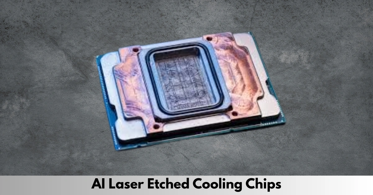
In the race to push computing power ever upward, especially for AI and data center workloads, heat remains a critical challenge. As chips become denser and more power hungry, traditional cooling methods like fans, cold plates, and immersion cooling are reaching their limits. That’s why Microsoft resorts to laser etching AI-designed cooling channels in chips, embedding microfluidic pathways directly into silicon to extract heat at its source. This innovative approach could transform thermal management in next-generation hardware, enabling more powerful, efficient, and reliable computing systems.
In this article, we’ll unpack what the technique involves, how Microsoft is applying it, the advantages and challenges, comparisons with traditional methods, and implications for the future of data center chip design.
Why Microsoft Is Pushing Into Embedded Cooling Channels
As AI workloads grow, so does the thermal pressure on GPUs, TPUs, and specialized AI accelerators. In its public announcement, Microsoft described how embedded microfluidic cooling can outperform standard cold plate cooling by up to three times, with up to 65% reduction in peak silicon temperature rise in lab tests.
The core idea, instead of cooling the chip from above (e.g., cold plates) or immersing it in fluid, routes coolant through microscopic channels etched directly into the chip substrate, bringing liquid much closer to the heat sources. This cuts out many layers of thermal resistance and grants a more precise, efficient path for heat removal.
Microsoft isn’t doing this alone. The company partnered with Swiss startup Corintis and used AI modeling to help derive the optimal layout of cooling channels, drawing inspiration from nature (e.g., leaf vein patterns) for efficient coolant flow.
How Laser Etching AI-Designed Cooling Channels Works
The Etching and Channel Fabrication
To build these microfluidic paths inside a chip, Microsoft uses laser etching techniques to cut narrow channels (often on the order of micrometers, sometimes no wider than a human hair) in the silicon substrate. These channels are aligned and optimized so coolant can flow close to hotspot regions—areas in the chip that generate the most heat (e.g. power delivery sections, compute cores, memory lanes).
Because these channels are embedded within the chip, the coolant interacts much more directly with the heat path, reducing thermal bottlenecks. In tests, Microsoft found that temperature peaks could be reduced by 65%, making the design up to 3× more efficient in cooling than cold plates.
AI-Driven Layout Optimization and Bio-Inspired Patterns
One challenge in designing these cooling channels is figuring out how to route coolant so that it flows where it’s needed most, without overly weakening the silicon structure. Microsoft uses AI models to analyze heat signatures on a chip (under expected workloads) and then propose channel patterns that best match thermal distribution. This sometimes results in branch-like, vein-like patterns resembling natural vascular systems.
These designs often outperform traditional straight up-down channel schemes because they balance fluid flow resistance and heat conduction paths more smartly.
Benefits Over Traditional Cooling Approaches
Efficiency and Temperature Reduction
By placing coolant paths so close to the heat source, Microsoft’s approach reportedly achieves up to 3× better heat removal versus standard cold-plate cooling in certain workloads. Peak temperatures in the silicon can be reduced by ~65%.
Lower silicon temperatures translate into several gains:
- Reduced thermal throttling, enabling the chip to maintain higher performance consistently
- Longer lifespan (less thermal stress on transistors)
- Less energy is spent on aggressive cooling systems
Density and Scalability
Better cooling enables tighter packing of chips (higher compute density) without overheating adjacent components. Microsoft sees this as critical for future data centers.
Moreover, because cooling is embedded, you can also cool stacked chip architectures (3D chip stacks) by etching channels in each layer before assembly. That helps overcome one of the main heat constraints that have limited realistic 3D stacking.
Energy & Sustainability Benefits
Because the coolant doesn’t have to be extremely cold to do its job (less thermal resistance to offset), Microsoft expects lower power consumption in cooling systems. That helps data centers improve Power Usage Effectiveness (PUE) and save on operational costs.
Also, heat that remains can more easily be repurposed (waste heat recovery) because the thermal gradient is closer to the source.
Challenges and Constraints
Manufacturing Complexity and Cost
Adding etched cooling channels into chips complicates the fabrication process. The etching must be extremely precise: too deep, and you weaken the silicon; too shallow, and cooling is ineffective. There’s little room for error.
Ensuring reliability (no leakage, no channel clogging, stable over time) is another hurdle. Packaging and sealing these microfluidic systems requires novel methods.
Consequently, early deployment is likely to favor premium data center chips or AI accelerators, rather than consumer GPUs or mass-market chips.
Thermal & Mechanical Design Trade-Offs
Balancing cooling effectiveness with structural integrity is not trivial. The chip design must accommodate cooling paths without violating mechanical or electrical constraints.
Channel clogging, coolant purity, fluid dynamics (pressure, flow rates), and maintenance over decades are also important considerations.
Integration and Ecosystem Readiness
This cooling method demands changes not just in chip design but in cooling infrastructure (how coolant is delivered, how leaks are prevented, how maintenance is done). Legacy data center systems would struggle to adopt it wholesale without large investment.
Additionally, industry partners (foundries, chip vendors) must support or adopt these changes, which could slow adoption.
Comparing Against Other Cooling Methods
| Cooling Technique | Advantages | Limitations / Trade-offs |
|---|---|---|
| Air cooling (fans, heatsinks) | Simple, cost-effective for low-power chips | Poor for high-density AI loads; thermally distant from hotspot |
| Cold plate / liquid cooling | Good for many high-power chips, well-understood | Multiple thermal interfaces reduce efficiency; less effective for 3D stacks |
| Immersion cooling | Uniform cooling, fewer hot spots | Complex infrastructure, potential reliability and compatibility issues |
| Embedded microfluidic cooling (Microsoft’s method) | Very high efficiency, minimal thermal lag, enables dense and 3D designs | Costly fabrication, reliability risks, and infrastructure complexity |
Because embedded channels physically bring liquid closer to where heat is generated, Microsoft’s method can surpass even advanced cold plates or immersion systems in terms of efficiency and temperature control, especially for the hottest chip zones.
However, for less demanding use cases (e.g., consumer PCs, low-power chips), the extra complexity may not yet be justified.
Looking Ahead | Implications for Chip Design & the Industry
Enabling New Architectures & Higher Power Density
With better embedded cooling, designers can push performance envelopes further—adding more cores, stacking dies, or increasing clock speeds. Thermal constraints are often among the most rigid limits in chip scaling; reducing that barrier opens new innovation pathways.
Embedded cooling also encourages heterogeneous stacking, where logic, memory, and accelerators can be stacked and cooled individually. This could accelerate 3D chip adoption.
Shift in Data Center Design & Density
Cooling is one of the limiting factors on how closely servers can be packed. Better cooling means tighter racks, smaller footprints, and more compute in the same datacenter volume.
Further, if this cooling method supports higher overclocking for bursts (e.g., during traffic peaks), fewer servers may be needed to handle load spikes—a big cost and carbon advantage.
Broader Industry Adoption & Standardization
Microsoft resorts to laser etching AI-designed cooling channels in chips, and intends to work with fabrication partners and broader industry players to transition this from a lab prototype to a deployable technology.
If adopted across the industry, we may see similar microfluidic cooling techniques in GPUs, AI accelerators, and eventually consumer chips—though that is likely years away.
Conclusion
In conclusion, laser-etched, AI-optimized cooling channels within chips represent a groundbreaking step toward solving the challenges of heat management in modern computing. While obstacles like fabrication complexity, cost, and integration remain, the potential for up to 3× better heat removal and significant temperature reductions could redefine hardware design, enabling denser, more powerful, and energy-efficient systems in the future.